Background
I was out picking up odds and ends from Walmart the other day, when I decided to check out the clearance aisle. Among a collection of products I could not care less about, I found a mini arcade game to play Tetris. I’ve seen these mini arcade cabinets before, usually paying them no mind. This time, however, a pertinent “what if” came to mind: what if I could change it to play something other than Tetris? And so, on a whim, I brought it home and got to work.
First Impressions
Surely I am not the first one to try something like this, so I made it a goal to not look anything up online that was specifically related to this toy (but general concepts are okay). I wanted to explore how hardware reverse engineering leads to software reverse engineering, where I am much more comfortable.
Obviously, the first thing I tried to do was play the game. Sadly, it came with dead batteries and even the batteries in my TV remote didn’t have enough juice to keep it powered for more than one second. I expected to need to buy some tools later, so AA batteries are on the list.
Nevertheless, the goal remained the same: I want to play a game that’s not Tetris using the same hardware.
Hardware Reverse Engineering
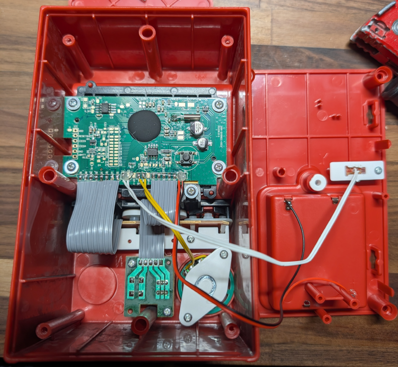
The next logical step was to take it apart. Fortunately, despite being a cheap toy, this step was easy. After removing four screws from each corner on the back of the cabinet, basically everything of interest is clearly visible.
What Am I Looking At?
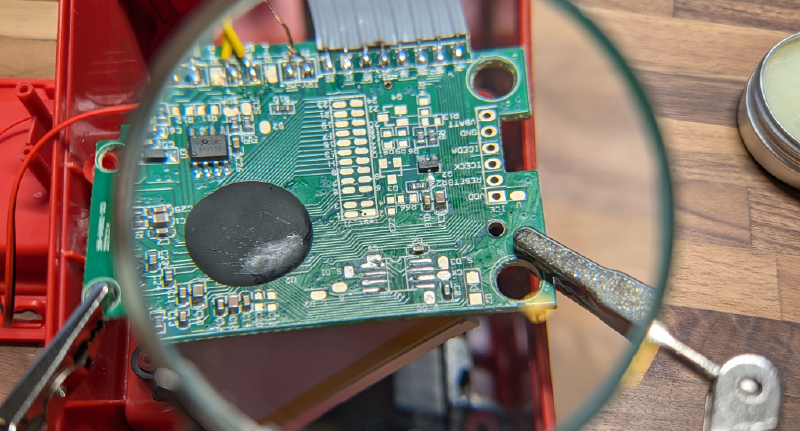
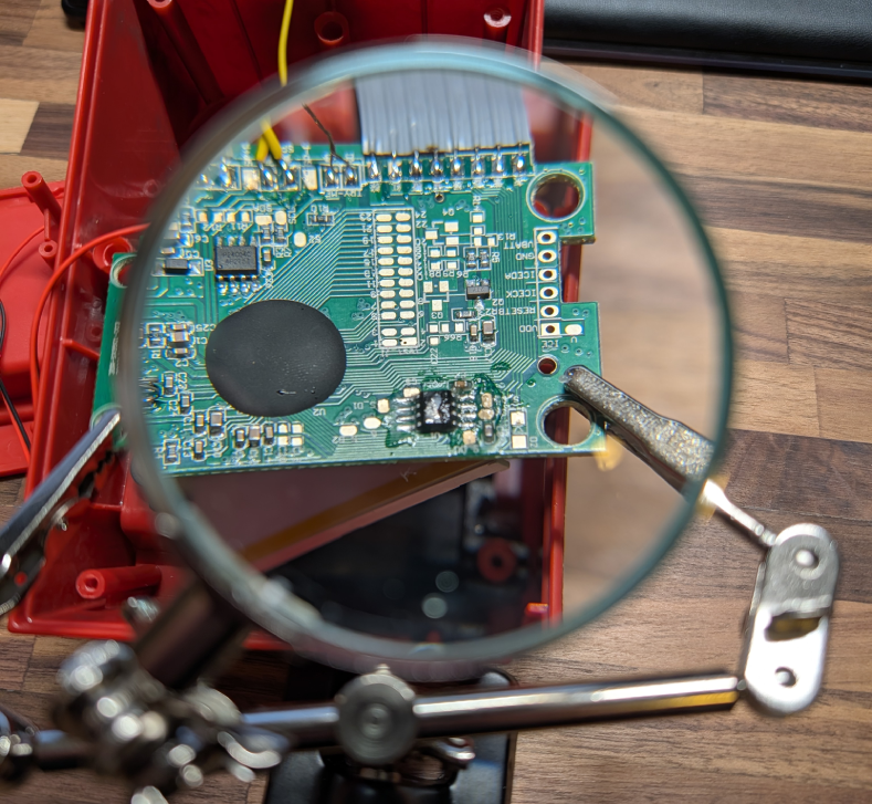
Being that I’m a novice at hardware RE, I figured a good first step is to write down all the identifiers for the components and look them up online. The idea being that knowing what a chip is responsible for helps me narrow down what I should be focusing on (for example, there’s no point taking a deep dive on a component that just distributes power). It’s at this stage that I learned the madness of the naming system actually serves a purpose. I won’t go into detail here, but I found this BusPriate Documentation to be very helpful.
There are only two chips on the board and one black blob:
| Component | Purpose |
|---|---|
| P24C04C | I2C EEPROM |
| MD25Q16C | SPI Flash EEPROM |
| Black Blob | Main SoC? |
The past version of me that just learned most those words could do very little with that information. So, I jumped the gun and bought some tools. My line of thinking was “if I can see what is active and when, then I can figure out what each component does.” Looking back, it would have been better to do a little more research, but I am now the proud own of a multimeter and a USB analyzer (and AA batteries).
Probing the Problem
One week later the tools arrived. I was still driven by the novelty of a new project at this point, and reached for the more interesting of the two tools: the USB analyzer. This allowed me to probe different parts of the board and visualize the signals in software like PulseView.
I decided to start by just firmly pressing jumper cables against different pads, looking for anything to show up on screen. The most interesting area on the board was around the MD25Q16C component, specifically a pad labeled CK. Signals from this pad would light up any time the game “did something” and be silent while the screen “waited.” For example, it would remain silent on the main menu unless some interaction was made.
At first, I attributed this to being responsible for playing sounds and video assets. But later I learned that is more likely that audio, video, and code are being read from the MD25Q16C component. Fortunately this style of memory is exceedingly common, making it easy to read the contents with the right tools.
A little research led me to purchase a CH341A Programmer despite some scary reviews claiming it can fry the chip during writes. I would also need a way to get components off and back onto the board, which the soldering iron I already own will do well enough.
As a side note, I was pleasantly surprised with the cost of all these tools. I was fully expecting to need a tool I simply couldn’t afford for work like this, but the tools I needed and didn’t own add up to only $30 USD so far! (the multimeter has been unused)
Desolder and Dump
Another week passed and more tools arrived. The process of dumping the data from a chip like this is seems to be most common in flashing a new bios onto laptops. Luckily the stakes here are much lower, but I can still benefit from the numerous guides online.
The easiest solution would have been to use the clip included with the programmer to read from the component while it was still soldered onto the board. Despite my best efforts, I could not get a good enough connection for flashrom to recognize the device. This led to the backup plan of desoldering the chip from the board, then placing it in the clip.
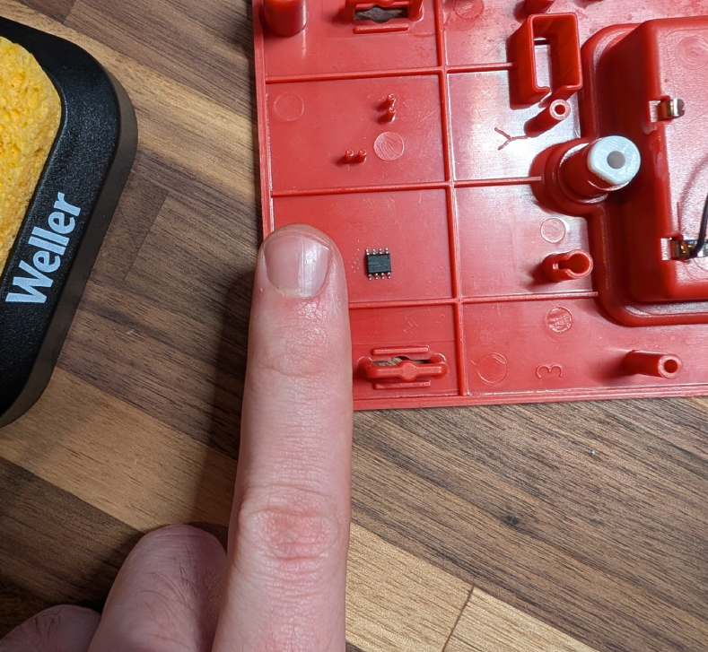
This was significantly more difficult than I was expecting. I started by applying flux to prepare to wick off as much solder as I could; the only problem was I don’t own solder wick. So, I did the next best thing by stripping a thick gauge wire and using that as my wick. Next, I heated up the pins with the soldering iron until the solder looked glossy and wicked away what I could. Repeating this on both sides of the component, I was able to remove a good amount of solder, but not enough to leave the component loose. Ultimately, I heated up all pins on one side of the component and gently lifted it with a pair of tweezers. This freed the legs on one side, so I repeated on the other.
All this work was done while looking through a magnifying glass. Once I looked at the chip without the magnification, it became clear why everything was so much more difficult than I thought: I could probably fit four components on one finger nail! This is far from the smallest component to exist, but it sure is tiny.
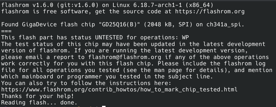
With the chip removed it was securely placed in the clip and I used flashrom to read all the contents. The only interesting thing of note here is that it was identified as flash chip “GD25Q16B” and not “MD25Q16C.” The last letter is just a revision, but the first two letters are usually the manufacturer. It’s possble that flashrom identifies all 25Q16 chips as manufactured by GigaDevice, but it’s also possible that this specific chip is a copy cat.
Software Reverse Engineering
With a dump file created, I am back in somewhat familiar territory. The contents of the dumped data are completely unknown. That means the format of any image or audio assets are also unknown. Then there’s the problem of the ISA for code. But this is all common for an embedded software problem.
Finding Audio Assets
Since the USB analyzer was showing activity when playing sounds, I decided to load the whole binary file into Audacity. The exact format is unknown, so I imported it as raw data with 8-bit PCM encoding, little endian, 1 channel, and 8000 Hz. The vast majority of the file are loud headache inducing sounds, but at the end there is the recognizable Tetris theme song. It’s what can only be described as “deep fried,” probably due to encoding issues, but it is recognizable. After tinkering with import options, the below results are from 16-bit PCM encoding, big endian, 1 channel, and 4000 Hz. There is still a lot of static and I’ve had to lower the volume to save the your eardrums.
Forcing myself to listen to the static disaster in the other parts of the file, there is also a recognizable countdown timer that occurs when starting a new game. Just before this there are additional sounds, but I can’t pinpoint their purpose.
Finding Image Assets
With the presence of “plaintext” audio, one can only assume that images can be recovered as well. For this, I used TileMolester (terrible name) and a lot of guess work. I started by loading the whole ROM into TileMolester using the 1bpp planer codec. I scrolled past the region I knew to be SFX but not all the way to the region I knew to be music. Then I adjusted the width until things “lined up” to reveal something that resembles the main menu of the game.
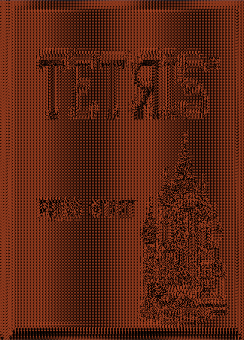
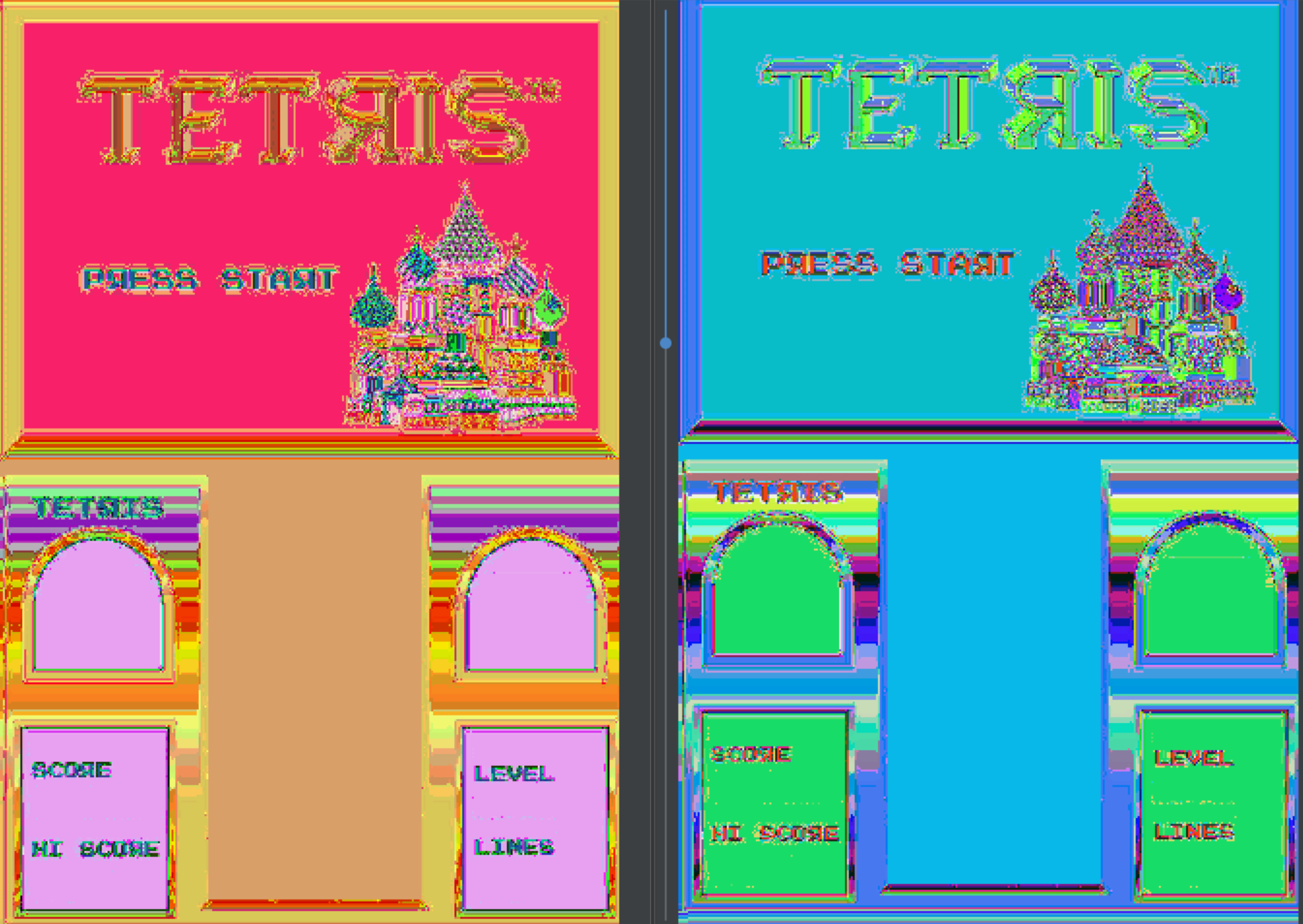
Much like the audio, the codec is wrong, leading to a barely recognizable image. Further guesswork led me to the 16bpp RGB codec and “2-Dimensional mode” for the clearest image. Given that the audio was more clear in big endian than little endian, I wrote a script to change the endian of the raw ROM dump. After applying the same settings, the image was even more clear than the non-swapped version. However, neither version is 100% correct and both have strange artifacts around edges. In addition to the main menu, options menu and the credits screen were also seen with similar quality.
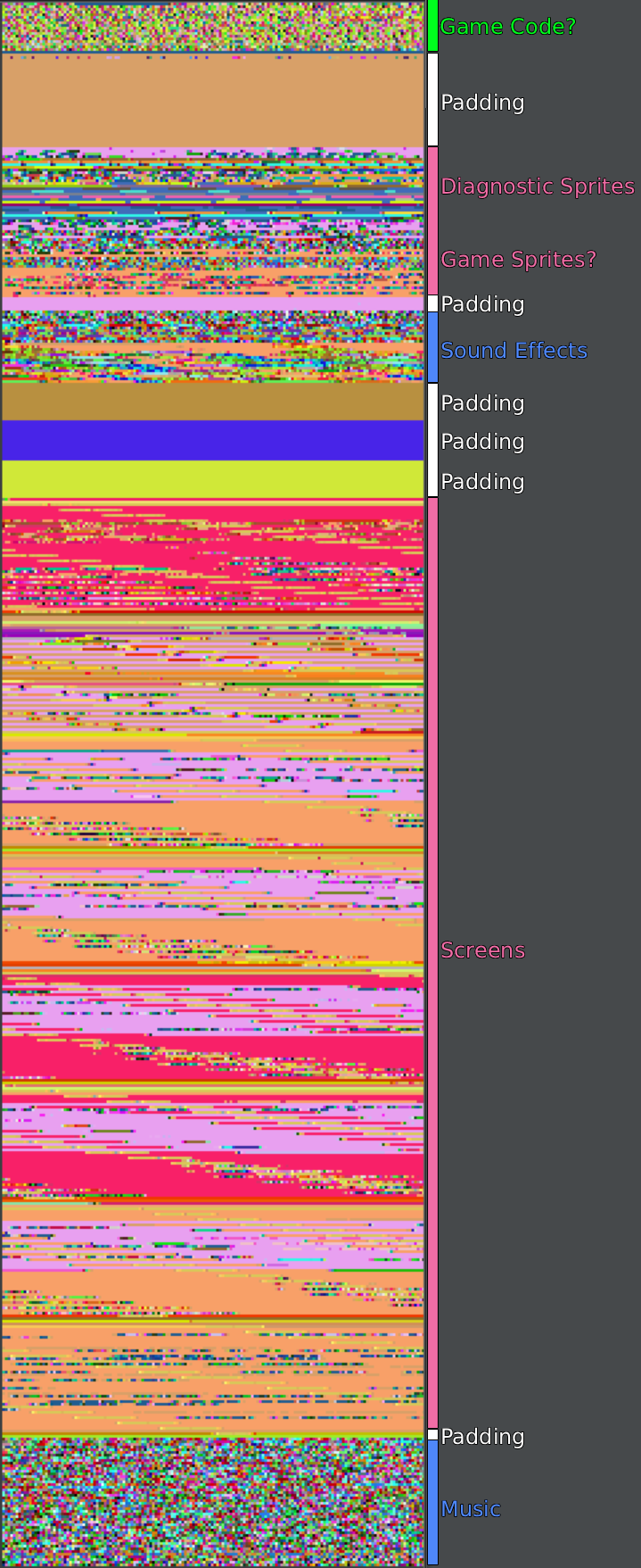
Images of the full screen are not originally what I intended to find. Instead, I was interested in locating the tetrimino sprites so that I could try changing their color. With a codec that is good enough, I scrubbed through the rest of the file looking for assets. Before the SFX there are a collection of what sprites that are visible by shrinking the width down significantly. From top to bottom they appear to be:
- Something I can’t quite figure out but might be an alphabet
- An isometric brick pattern in several colors
- Diagnostic messages: BATT FAIL, PASS, Single, Checksum, Not Found
- Directional arrows in several colors
- Circles in several colors
- Rounded squares in several colors
- Swirly arrows in several colors
- Tetriminos
- Two more things I can’t figure out

The presence of diagnostic messages worries me, specifically the “Checksum” message. A signature check makes the low hanging fruit of changing the tetrimino colors much more difficult, since it may require the game code to be reverse engineered.
Finding Code
With sprites, sound effects, screens, and music found, all that remains is the code. This step was actually made easy due to the format of the ROM. All remaining sections of ROM have extremely low entropy except for one: the very beginning. In fact, using TileMolester gives a somewhat interesting overview of the file format.
I tried importing the code into Ghidra using every big endian variant of the supported 16-bit architectures, but they all failed to disassemble in different ways. The most likely reason is that Ghidra doesn’t support this architecture, but maybe someone wrote a Sleigh file I can download. More research will need to go into finding the correct architecture and how to get it loaded in Ghidra.
Possible Encryption
As I finished writing everything above (and below), I realized that the images bear a striking resemblance to the ECB penguin. While I am able to recover audio and image assets, it’s entirely possible that they are not plaintext, but are poorly encrypted.
Whether this is true or not will be revealed once the architecture and instruction set (ISA) are known; even poor encryption will stop me in my tracks from static reverse engineering after I have the ISA correct.
Next Steps
My grand idea of getting this toy to run something other than Tetris is becoming less and less likely. Moving forward, I will not be limiting myself by not looking at existing work on this subject. I will allow myself to find resources pertaining to BasicFun products in general, but not their Tetris game specifically.
Sadly, in my rush to try flashing the chip to see if I could trigger a checksum error, I accidentally snapped a leg off the chip when removing it from its clip. More (hopefully) compatible chips are on the way, but will take a few more weeks before they arrive.
In the meantime, I’m left to consider one software question and one hardware question:
- What is the architecture of the black blob chip?
- How can I wire up the SPI flash EEPROM chip in a way that I won’t keep breaking them?
That concludes the first part of this adventure. I would usually wait until I’m finished to share the story, but this website might get more traffic soon since it’s how I am credited as an author for the CrackMes One CTF 2026. For those participating, this blog post may help you get started. Or maybe the writeups for my WeeperVM – Level 1 and WeeperVM – Level 2 challenges will tip you off to how I forward engineer. Good luck!